
An optional part of the ARMv7-M architecture is the support of a Memory Protection Unit (MPU). This is a fairly simplistic device (compared to a fully blow Memory Management Unit (MMU) as found on the Cortex-A family), but if available can be programmed to help capture illegal or dangerous memory accesses.
When first looking at programming the MPU it may seem rather daunting, but in reality it is very straightforward. The added benefit of the ARMv7-M family is the well-defined memory map.
All example code is based around an NXP LPC1768 and Keil uVision v4.70 development environment. However as all examples are built using CMSIS, then they should work on an Cortex-M3/4 supporting the MPU.
First, let’s take four types of memory access we may want to capture or inhibit:
- Tying to read at an address that is reserved in the memory map (i.e. no physical memory of any type there)
- Trying to write to Flash/ROM
- Stopping areas of memory being accessible
- Disable running code located in SRAM (eliminating potential exploit)
Before we start we need to understand the microcontrollers memory map, so here we can look at the memory map of the NXP LPC1768 as defined in chapter 2 of the LPC17xx User Manual (UM10360).
- 512kB FLASH @ 0x0000 0000 – 0x0007 FFFF
- 32kB on-chip SRAM @ 0x1000 0000 – 0x1000 7FFFF
- 8kB boot ROM @ 0x1FFF 0000 – 0x1FFF 1FFF
- 32kB on-chip SRAM @ 0x2007 C000 [AHB SRAM]
- GPIO @ 0x2009C000 – 0x2009 FFFF
- APB Peripherals @ 0x4000 0000 – 0x400F FFFF
- AHB Peripheral @ 0x5000 0000 – 0x501F FFFF
- Private Peripheral Bus @ 0xE000 0000 – 0xE00F FFFF
Based on the above map we can set up four tests:
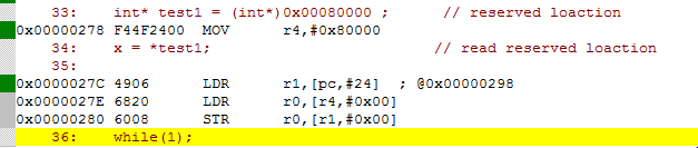
- Read from location 0x0008 0000 – this is beyond Flash in a reserved area of memory
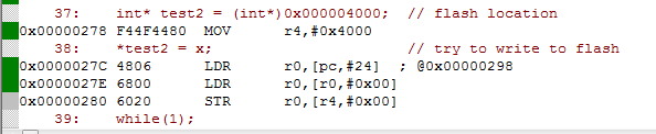
- Write to location 0x0000 4000 – some random loaction in the flash region
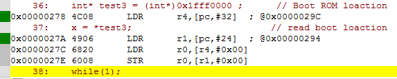
- Read the boot ROM at 0x1FFF 0000
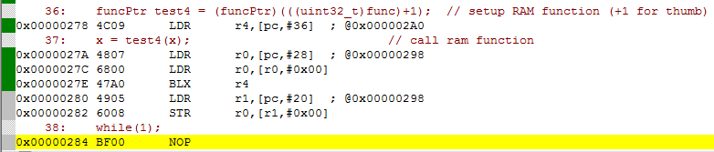
- Construct a function in SRAM and execute it
The first three tests are pretty easy to set up using pointer indirection, e.g.:
int* test1 = (int*)0x000080000;   // reserved location
x= *test1;                        // try to read from reserved location
int* test2 = (int*)0x000004000;   // flash location
*test2 = x;                       // try to write to flash
int* test3 = (int*)0x1fff0000 ;   // Boot ROM location
x = *test3 ;                      // try to read from boot ROM
The fourth takes a little more effort, e.g.
// int func(int r0)
// {
//    return r0+1;
// }
uint16_t func[] = { 0x4601, 0x1c48, 0x4770 };
int main(void)
{
   funcPtr test4= (funcPtr)(((uint32_t)func)+1);  // setup RAM function (+1 for thumb)
   x = test4(x);                                  // call ram function
   while(1);
}
Contents
Default Behavior
Without the MPU setup the following will happen (output from the previous Fault Handler project):
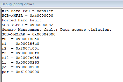
- test1 will generate a precise bus error
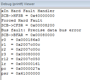
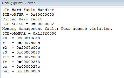
- test2 will generate an imprecise bus error
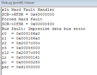
Test3 and test4 will run without any fault being generated.
Setting up the MPU
There are a lot of options when setting up the MPU, but 90% of the time a core set are sufficient. The ARMv7-M MPU supports up to 8 different regions (an address range) that can be individually configured. For each region the core choices are:
- the start address (e.g. 0x10000000)
- the size (e.g. 32kB)
- Access permissions (e.g. Read/Write access)
- Memory type (here we’ll limit to either Normal for Flash/SRAM, Device for NXP peripherals, and Strongly Ordered for the private peripherals)
- Executable or not (refereed to a Execute Never [XN] in MPU speak)
Both access permissions and memory types have many more options than those covered here, but for the majority of cases these will suffice. Here I’m not intending to cover privileged/non-privileged options (don’t worry if that doesn’t make sense, I shall cover it in a later posting).
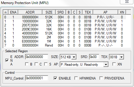
Based on our previous LPC1768 memory map we could define as region map thus:
No.  Memory             Address       Type      Access Permissions  Size
0    Flash              0x00000000    Normal    Full access, RO    512KB
1    SRAM               0x10000000    Normal    Full access, RW     32KB
2    SRAM               0x2007C000    Normal    Full access, RW     32KB
3    GPIO               0x2009C000    Device    Full access, RW     16KB
4    APB Peripherals    0x40000000    Device    Full access, RW    512KB
5    AHB Peripherals    0x50000000    Device    Full access, RW      2MB
6    PPB                0xE0000000    SO        Full access, RW      1MB
Not that the boot ROM has not been explicitly mapped. This means any access to that region once the MPU has been initialized will get caught as a memory access violation.
To program a region, we need to write to two registers in order:
- MPU Region Base Address Register (CMSIS: SCB->RBAR)
- MPU Region Attribute and Size Register (CMSIS: SCB->RASR)
MPU Region Base Address Register
Bits 0..3 specify the region number
Bit 4 needs to be set to make the region valid
bits 5..31 have the base address of the region (note the bottom 5 bits are ignored – base address must also be on a natural boundary, i.e. for a 32kB region the base address must be a multiple of 32kB).
So if we want to program region 1 we would write:
#define VALID 0x10

SCB->RBAR = 0x10000000 | VALID | 1;  // base addr | valid | region no
MPU Region Attribute and Size Register
This is slightly more complex, but the key bits are:
bit 0 – Enable the region
bits 1..5 – region size; where size is used as 2**(size+1)
bits 16..21 – Memory type (this is actually divided into 4 separate groups)
bits 24..26 – Access Privilege
bit 28 – XN
So given the following defines:
#define REGION_Enabled  (0x01)
#define REGION_32K      (14 << 1)      // 2**15 == 32k
#define NORMAL          (8 << 16)      // TEX:0b001 S:0b0 C:0b0 B:0b0
#define FULL_ACCESS     (0x03 << 24)   // Privileged Read Write, Unprivileged Read Write
#define NOT_EXEC        (0x01 << 28)   // All Instruction fetches abort
We can configure region 0 thus:
SCB->RASR = (REGION_Enabled | NOT_EXEC | NORMAL | REGION_32K | FULL_ACCESS);
We can now repeat this for each region, thus:
void lpc1768_mpu_config(void)
{
   /* Disable MPU */
   MPU->CTRL = 0;
   /* Configure region 0 to cover 512KB Flash (Normal, Non-Shared, Executable, Read-only) */
   MPU->RBAR = 0x00000000 | REGION_Valid | 0;
   MPU->RASR = REGION_Enabled | NORMAL | REGION_512K | RO;
   /* Configure region 1 to cover CPU 32KB SRAM (Normal, Non-Shared, Executable, Full Access) */
   MPU->RBAR = 0x10000000 | REGION_Valid | 1;
   MPU->RASR = REGION_Enabled | NOT_EXEC | NORMAL | REGION_32K | FULL_ACCESS;
   /* Configure region 2 to cover AHB 32KB SRAM (Normal, Non-Shared, Executable, Full Access) */
   MPU->RBAR = 0x2007C000 | REGION_Valid | 2;
   MPU->RASR = REGION_Enabled | NOT_EXEC | NORMAL | REGION_32K | FULL_ACCESS;
   /* Configure region 3 to cover 16KB GPIO (Device, Non-Shared, Full Access Device, Full Access) */
   MPU->RBAR = 0x2009C000 | REGION_Valid | 3;
   MPU->RASR = REGION_Enabled |DEVICE_NON_SHAREABLE | REGION_16K | FULL_ACCESS;
   /* Configure region 4 to cover 512KB APB Peripherials (Device, Non-Shared, Full Access Device, Full Access) */
   MPU->RBAR = 0x40000000 | REGION_Valid | 4;
   MPU->RASR = REGION_Enabled | DEVICE_NON_SHAREABLE | REGION_512K | FULL_ACCESS;
   /* Configure region 5 to cover 2MB AHB Peripherials (Device, Non-Shared, Full Access Device, Full Access) */
   MPU->RBAR = 0x50000000 | REGION_Valid | 5;
   MPU->RASR = REGION_Enabled | DEVICE_NON_SHAREABLE | REGION_2M | FULL_ACCESS;
   /* Configure region 6 to cover the 1MB PPB (Privileged, XN, Read-Write) */
   MPU->RBAR = 0xE0000000 | REGION_Valid | 6;
   MPU->RASR = REGION_Enabled |STRONGLY_ORDERED_SHAREABLE | REGION_1M | FULL_ACCESS;
   /* Enable MPU */
   MPU->CTRL = 1;
   __ISB();
   __DSB();
}
After the MPU has been enabled, ISB and DSB barrier calls have been added to ensure that the pipeline is flushed and no further operations are executed until the memory access that enables the MPU completes.
Using the Keil environment, we can examine the MPU configuration:
Rerunning the tests with MPU enabled
To get useful output we can develop a memory fault handler, building on the Hard Fault handler, e.g.
void printMemoryManagementErrorMsg(uint32_t CFSRValue)
{
   printErrorMsg("Memory Management fault: ");
   CFSRValue &= 0x000000FF; // mask just mem faults
   if((CFSRValue & (1<<5)) != 0) {
      printErrorMsg("A MemManage fault occurred during FP lazy state preservation\n");
   }
   if((CFSRValue & (1<<4)) != 0) {
      printErrorMsg("A derived MemManage fault occurred on exception entry\n");
   }
   if((CFSRValue & (1<<3)) != 0) {
      printErrorMsg("A derived MemManage fault occurred on exception return.\n");
   }
   if((CFSRValue & (1<<1)) != 0) {
      printErrorMsg("Data access violation.\n");
   }
   if((CFSRValue & (1<<0)) != 0) {
      printErrorMsg("MPU or Execute Never (XN) default memory map access violation\n");
   }
   if((CFSRValue & (1<<7)) != 0) {
      static char msg[80];
      sprintf(msg, "SCB->MMFAR = 0x%08x\n", SCB->MMFAR );
      printErrorMsg(msg);
   }
}
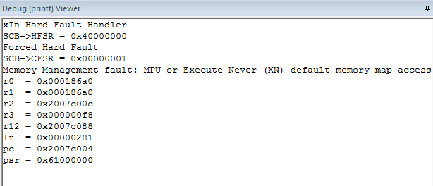
Test 1 – Reading undefined region
Rerunning test one with the MPU enabled gives the following output:
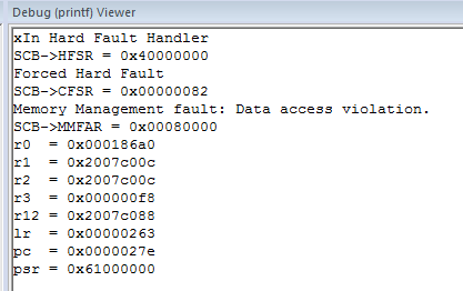
The SCB->MMFAR contains the address of the memory that caused the access violation, and the PC guides us towards the offending instruction
Test 2 – Writing to RO defined region
Test 3 – Reading Undefined Region (where memory exists)
Test 4 – Executing code in XN marked Region
The PC gives us the location of the code (in SRAM) that tried to be executed
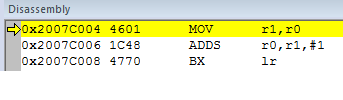
The LR indicates the code where the branch was executed
So, we can see with a small amount of programming we can (a) simplify debugging by quickly being able to establish the offending opcode/memory access, and (b) better defend our code against accidental/malicious access.
Optimizing the MPU programming.
Once useful feature of the Cortex-M3/4 MPU is that the Region Base Address Register and Region Attribute and Size Register are aliased three further times. This means up to 4 regions can be programmed at once using a memcpy. So instead of the repeated writes to RBAR and RASR, we can create configuration tables and initialize the MPU using a simple memcpy, thus:
uint32_t table1[] = {
/* Configure region 0 to cover 512KB Flash (Normal, Non-Shared, Executable, Read-only) */
(0x00000000 | REGION_Valid | 0),
(REGION_Enabled | NORMAL_OUTER_INNER_NON_CACHEABLE_NON_SHAREABLE | REGION_512K | RO),
/* Configure region 1 to cover CPU 32KB SRAM (Normal, Non-Shared, Executable, Full Access) */
(0x10000000 | REGION_Valid | 1),
(REGION_Enabled | NOT_EXEC | NORMAL | REGION_32K | FULL_ACCESS),
/* Configure region 2 to cover AHB 32KB SRAM (Normal, Non-Shared, Executable, Full Access) */
(0x2007C000 | REGION_Valid | 2),
(REGION_Enabled | NOT_EXEC | NORMAL_OUTER_INNER_NON_CACHEABLE_NON_SHAREABLE | REGION_32K | FULL_ACCESS),
/* Configure region 3 to cover 16KB GPIO (Device, Non-Shared, Full Access Device, Full Access) */
(0x2009C000 | REGION_Valid | 3),
(REGION_Enabled | DEVICE_NON_SHAREABLE | REGION_16K | FULL_ACCESS)
};

uint32_t table2[] = {
/* Configure region 4 to cover 512KB APB Peripherials (Device, Non-Shared, Full Access Device, Full Access) */
(0x40000000 | REGION_Valid | 4),
(REGION_Enabled | DEVICE_NON_SHAREABLE | REGION_512K | FULL_ACCESS),
/* Configure region 5 to cover 2MB AHB Peripherials (Device, Non-Shared, Full Access Device, Full Access) */
(0x50000000 | REGION_Valid | 5),
(REGION_Enabled | DEVICE_NON_SHAREABLE | REGION_2M | FULL_ACCESS),
/* Configure region 6 to cover the 1MB PPB (Privileged, XN, Read-Write) */
(0xE0000000 | REGION_Valid | 6),
(REGION_Enabled | NOT_EXEC | DEVICE_NON_SHAREABLE | REGION_1M | P_RW_U_NA),
};

void lpc1768_mpu_config_tbl(void)
{
   /* Disable MPU */
   MPU->CTRL = 0;
   memcpy((void*)&( MPU->RBAR), table1, sizeof(table1));
   memcpy((void*)&( MPU->RBAR), table2, sizeof(table2));
   /* Enable MPU */
   MPU->CTRL = 1;
   __ISB();
   __DSB();
}
I hope this is enough to get you started with your ARMv7-M MPU.
Niall has been designing and programming embedded systems for over 30 years. He has worked in different sectors, including aerospace, telecomms, government and banking.
His current interest lie in IoT Security and Agile for Embedded Systems.
- Navigating Memory in C++: A Guide to Using std::uintptr_t for Address Handling - February 22, 2024
- Embedded Expertise: Beyond Fixed-Size Integers; Exploring Fast and Least Types - January 15, 2024
- Disassembling a Cortex-M raw binary file with Ghidra - December 20, 2022
Co-Founder and Director of Feabhas since 1995.
Niall has been designing and programming embedded systems for over 30 years. He has worked in different sectors, including aerospace, telecomms, government and banking.
His current interest lie in IoT Security and Agile for Embedded Systems.
Thank you, very interesting!
Excellent, helpful post on one of the most under-rated and under-utilized parts of most Cortex M3 & M4s. Thank you.
Well written. Thank you for posting. I work for NXP. Please consider posting to the LPCware site.
There is a typo in first line of first snippet :
0x000004000; // reserved location
instead of
0x00080000; // reserved location
Thanks, amazing it's been there for four years and you're the first to spot it!
This post is great, im testing MPU of stm32l152 board with gnuGcc +eclipse. Thanks for your help in this topic!
Hi, thank you for the tutorial. Before finding your post, I watched an STM32 tutorial using a different board and decided to get it. How different is the code for the stm32 keil tutorial? My board has the STM32F0 controller.
Thanks,
Alex
Hi Alex,
Assuming you processor does have an MPU the the basic code should work. The differences will be in the Flash/RAM sizes. Without checking I don't think the STM32F0's have an MPU.
Niall.
I'm looking for a method to setup the MPU for protection against NULL-pointer dereferencing. The presented MPU setup protects against writing to the NULL-pointer (as a side effect of configuring the Flash ROM region as read-only). But how about the *reads* from NULL-pointer? How to set that up? I understand that it might conflict with the vector table (also at address 0x0). Any help will be highly appreciated!
Hi Samek,
In theory, I think it should be possible. In pretty much all Cortex-M cores I'm working with, the actual Flash is remapped, so only appears at Zero(0) on power-up. So this shouldn't be an issues for MPU setup. My only concern is whether the MPU is still in operation for soft/debug type resets - this might pose an issue. I'll have to dig deeper.
I'll try and have a play, but I'm teaching for the next couple of weeks, so it probably won't be until nearer Xmas!
Best regards,
Niall.
Hi Miro and Niall,
As Niall said, most CM 3 / 4 / 7 MCUs (actually, all that I work with) re-map the flash after boot, for example on the STM32 MCUs, generally speaking, the flash gets mapped (after reset fetch etc.) to 0x0800.0000. So in fact no access, read or write, to address 0 (e.g. read or write through a null ptr) would make sense.
"All" you need to do is not map that region of memory. Then any access to it will generate an MPU fault.
Perhaps you know this already, but note that the MPU also has a setting for default or "background" accesses (this is the PRIVDEFENA bit in the control register) -- what happens when an access to an unmapped region is attempted when running privileged (much embedded software always runs privileged, as I know you know...). When this bit is 0, if I recall correctly, any access to an unmapped region will result in a fault. If it is set to 1, the "background" (default / POR) rules are in place, which is obviously going to be chip-specific.
(Also, my recollection is that across a reset (e.g. when debugging and the debugger is requested to reset the CPU) all registers go back to their default values. I think this is probably also chip- and deugger-specific though.)
You know how to reach me if you'd like to discuss further.
P.S. Niall, I am on the opposite end of your situation, I just finished 2 weeks of training and it feels good to be freed up.
Hi Niall and Dan,
Thanks a lot for the suggestions. Indeed, for MCUs that do the Flash remap away from address 0x0 (like STM32), the simple MPU setup works and catches NULL-pointer dereferencing (both reads and writes).
Here is the code (similar to what I've posted in my [question on StackOverflow](https://stackoverflow.com/questions/74549991/null-pointer-protection-with-arm-cortex-m-mpu)):
```
/* Configure region 7 */
MPU->RBAR = 0x00000000U
| MPU_RBAR_VALID_Msk
| (MPU_RBAR_REGION_Msk & 7U);
MPU->RASR = (9 << MPU_RASR_SIZE_Pos) /* 2**(9+1) region */
| (0x0 <CTRL = MPU_CTRL_PRIVDEFENA_Msk | MPU_CTRL_ENABLE_Msk;
__ISB();
__DSB();
```
But for MCUs that don't perform the remap, such as Tiva or LPC, the Vector Table needs to be additionally relocated (otherwise the MPU blocks the access to the vectors). With the Vector Table relocated the MPU setup works fine. One needs to be only careful to size the region so that it does not overlap the relocated VT.
Finally, I had trouble with the EFM32 where the MPU setup did NOT catch NULL-pointer dereferencing. (Again, EFM32 required relocating the VT, but this didn't seem to be a problem).
--Miro